High Volume
Memory Test
Increased data consumption and the growing proliferation of memory device applications are driving the demand for DRAM and Flash memory. FormFactor production wafer probe cards offer cost-effective solutions for memory test.
In addition to smartphones and other portable devices, memory IC applications have expanded into data centers, solid state drives (SSDs), automobiles, appliances, and other electronics.
As the memory IC market continues to advance and expand, semiconductor manufacturers face the complex challenges of high parallelism, full-wafer contact testing. FormFactor’s range of high-performance wafer test solutions help chip suppliers achieve yield optimization, lower cost of test and faster time-to-market for today’s advanced memory devices.
DRAM - Full-wafer Contact Testing
Targeting 1-2 Touchdowns with 256-3200 Sites
The DRAM technology process nodes continue to shrink, driven by the demand to increase bit density and reduce memory device cost. With the recent accelerated transition to the 1Z and 1α nanometer process nodes, die count per wafer is increasing rapidly. As a result, full-wafer DRAM probe cards that simultaneously test every die on the wafer must keep pace with this increase. In addition, wafer sort throughput must advance to achieve the target cost without adding significant capital expenditure to the existing test floor.
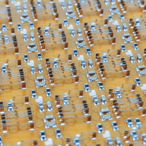
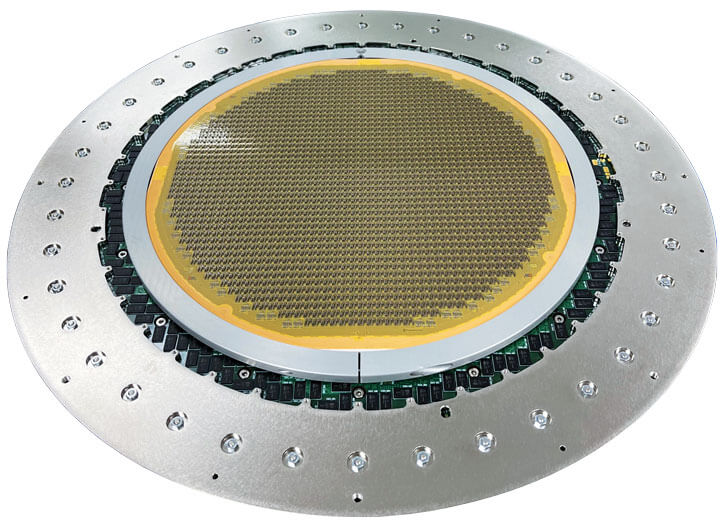
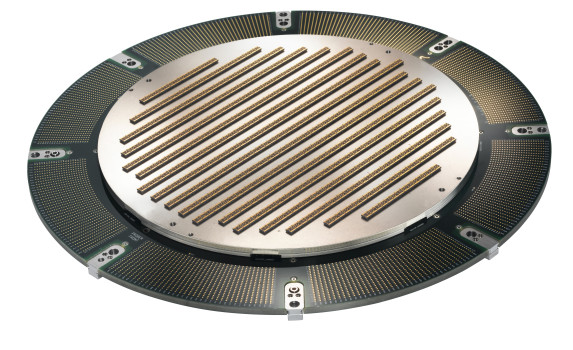
Working with the world’s largest memory manufacturers, FormFactor is the leader in developing and qualifying next generation DRAM probe cards. FormFactor’s SmartMatrix 3000XP probe card solution incorporates custom electronics to enhance signal integrity while leveraging massive tester resource sharing to enable highly parallel test at the 1Z and 1α nanometer nodes. Specifically developed to support fast design ramps and advanced product roadmaps, this platform extends the production-proven Matrix™ architecture to provide test parallelism in excess of 3000 die per wafer on a single touchdown. Unique technology features enable FormFactor’s Matrix platform to support challenging test requirements.
ATRE
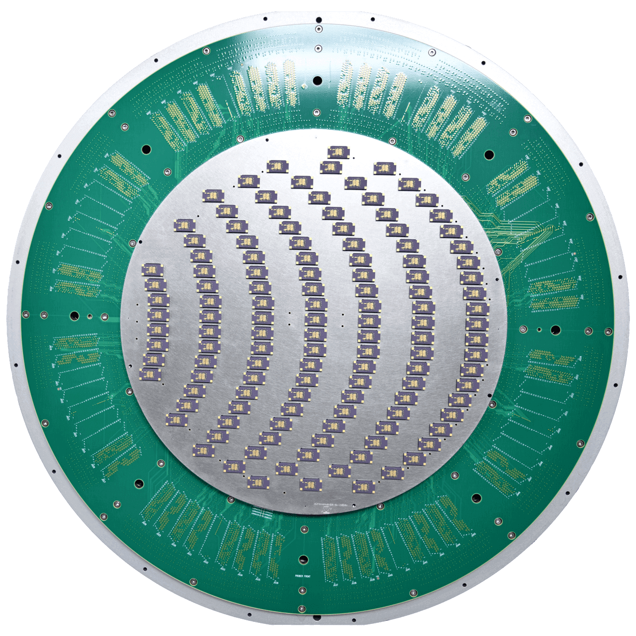
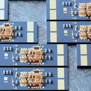
FormFactor’s ATRE (Advanced Tester Resource Enhancement) is a collection of custom devices and corresponding infrastructure that enables high parallelism test by increasing native tester resources controlled by the test program through customized communication protocols.
Next Generation KGD and High-Speed Memory Test for Advanced Packages
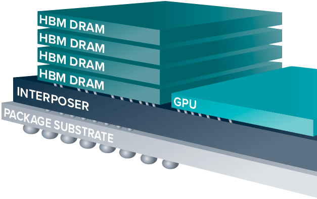
Recent industry-wide adoption of heterogeneous integrated systems enabled by 2.5D and 3D advanced packaging technology is driving up the demand for known-good-die (KGD). The KGD benefit ensures the final stacked and assembled package does not get scrapped due to one bad chip, effectively improving the final yield and reducing the cost of packaging.
As the demand for advanced package IC’s dramatically increases, KGD test solutions require better test efficiency to reduce cost and support higher volume. Coupled with the advancement of DRAM and High Bandwidth Memory (HBM) native speed capability, the latest memory is running beyond 2 GHz (4 Gbps) which is pushing the limit on existing ATE testers. Recent joint efforts between FormFactor and industry leaders successfully demonstrated that testing beyond 3 GHz is achievable.
The extended capability of FormFactor’s HFTAP K32 probe card solution enables DRAM customers on wafer-level speed testing up to 3.2 GHz/ 6.4 Gbps for next-generation KGD memory. This advanced MEMS probe card is used to verify electrical performance and yield, not only for the individual chips, but also devices used in the HBM stack, including the fine-pitch interposer to ensure the performance of the complete package.
Utilizing the production proven SmartMatrix platform, the HFTAP K32 probe card solution is capable of operating at a wide temperature range. The HFTAP K32 empowers customers to gain more intelligence at any stage of the heterogeneous integration process, where traditional methods to optimize yield on a monolithic silicon die are no longer adequate.
Flash — Full-wafer Contact NAND/NOR Flash Probing
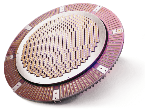
The Genus probe card is FormFactor’s newest 300 mm full-wafer contact testing solution for NAND Flash applications. The product enables one touchdown capability for NAND Flash testing with high pin count capability addressing the industry’s drive to increase bit growth and complexity. The ability to increase pin counts results in improved power delivery for 3D NAND with additional power and ground pins.
Using FormFactor’s proven 2D MEMS probes and space transformation technology, the Genus platform delivers optimum CTE matching for a wide temperature range, resulting in optimized probe placement and superior scrub performance. The Genus probe family offers dual temperature capability of -40°C to 130°C. Genus allows fast time to market to meet critical first silicon needs.
For high pin count, high speed NOR Flash testing, FormFactor’s TouchMatrix product offers a wafer probe solution designed specifically to deliver the lowest overall test cost per die for 200 mm and 300 mm NOR Flash wafer testing. It provides massive parallelism and adjusts to variations in manufacturers’ test equipment and product designs, to optimize probe planarity and speed set-up. Together, these features improve productivity and reduce the total cost of ownership.
